
Image courtesy of Dr. Aaswath Raman
“The methods we’ve developed are an important step towards global photonics and materials design strategies that can identify combinations of device categories, material properties and geometric parameters, which algorithmically deliver a sought functionality”
– Dr. Aaswath Raman
Materials scientists at the UCLA Samueli School of Engineering have developed a new way to optimize the design of complex optical materials by using the same machine-learning technique that creates deceptive imagery known as “deepfakes.” Instead, the advance can be leveraged for positive scientific breakthroughs, including a broad range of new devices, such as more efficient solar panels or faster microchip components.
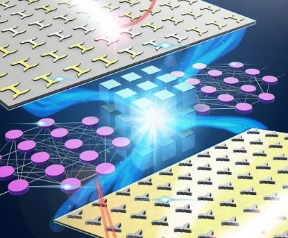
Optical materials are used to control how light absorbs, reflects, focuses and more. The researchers’ new approach incorporates three variables: materials’ optical properties, such as their refractive index; their three-dimensional geometry and how building block pieces can fit for assembly; and the category of device itself. A research paper on the breakthrough was recently published in Advanced Optical Materials and featured on the front cover of the journal.
“Currently, it is very computationally difficult to design complex optical materials, such as metamaterials or nanophotonic devices, when there’s a specific target response being sought. There are too many variables for an easy path toward the best solutions,” said Aaswath Raman, a UCLA assistant professor of materials science and engineering who led the research. “This method allows us to step back and treat this complex materials design challenge as an image-generation problem. It harnesses the power of machine-learning technology already used in imaging and reconfigures it for materials design and optimization.”
The researchers used a class of image-based, deep machine-learning models called generative adversarial networks, or GANs. GANs have been used to create deepfakes — stunningly real-looking, digitally altered images and videos that can bring a famous portrait to life or mimic a celebrity’s appearance. Inspired by GANs’ ability to encode and work with large quantities of variable data, the researchers instead use the models to generate accurate materials design.
“What we’ve done in our computational model is replacing all the image data, like colors and pixels, with various physical properties of materials and their corresponding nanoscale structural elements,” said Christopher Yeung, a materials science doctoral student at UCLA who is the first author on the paper. “We then trained it to home in on a particular type of device we wanted to build. For example, if we want a nanoscale optical component that only absorbs a certain band of infrared light, this technique can tell us the best combination of materials and geometries to build such a device.”
In addition, the team found that the GANs could produce multiple design variants for the same desired outcome using different materials and structures. This could give materials designers more options from which to choose, considering factors such as cost and availability of materials.
In their experiments, the researchers also demonstrated that their framework can work with publicly available material databases to bring to fruition more new designs predicted by machine learning.
“The methods we’ve developed are an important step towards global photonics and materials design strategies that can identify combinations of device categories, material properties and geometric parameters, which algorithmically deliver a sought functionality,” Raman said.
Other authors on the paper include Ryan Tsai, a high school student who interned with Raman’s research group; UCLA undergraduates Benjamin Pham, Brian King and Julia Liang; visiting graduate student Yusaku Kawagoe; UCLA graduate student David Ho; and Mark W. Knight from Northrop Grumman Corporation.
The research was supported by a Sloan Research Fellowship awarded to Raman from the Alfred P. Sloan Foundation.